
PN Junction, Forward Bias, Reverse Bias
PN Junction:
When a p-type semiconductor is suitably joined to an n-type semiconductor, the contact surface is called a PN junction.
Function of PN Junction:
At the instant of PN-junction formation, the free electrons near the junction in the n region begin to diffuse across the junction into the p region where they combine with holes near the junction. The result is that the n region loses free electrons as they diffuse into the junction. This creates a layer of positive charges (pentavalent ions) near the junction. As the electrons move across the junction, the p region loses holes as the electrons and holes combine. The result is that there is a layer of negative charges (trivalent ions) near the junction. These two positive and negative charge layers form the depletion region (or depletion layer). The term depletion is because, near the junction, the region is depleted (i.e. emptied) of charge carriers (free electrons and holes) due to diffusion across the junction. It may be noted that the depletion layer is formed very quickly and is very thin compared to the n region and the p region.
For clarity, the width of the depletion layer is shown to be exaggerated.
Once the PN junction is formed and the depletion layer is created, the diffusion of free electrons stops. In
other words, the depletion region acts as a barrier to the further movement of free electrons across the
junction. The positive and negative charges set up an electric field. The electric field is a barrier to the free electrons in the n-region. There exists a potential
difference across the depletion layer which is called barrier potential (V0
). The barrier potential of a PN junction depends upon several factors including the type of semiconductor material, the amount of
doping, and temperature. The typical barrier potential is approximately:
For silicon, V0
= 0.7 V ; For germanium, V0
= 0.3 V
For an electronic device. About a PN junction, there are the following two bias conditions:
1. Forward biasing 2. Reverse biasing
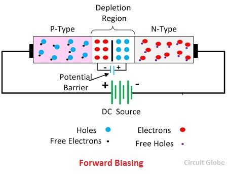
Forward Biasing:
When external D.C. voltage applied to the junction is in such a direction
that it cancels the potential barrier, thus permitting current flow, it is called forward bias.
To apply forward bias, connect the positive terminal of the battery to the p-type and the negative terminal to the n-type.
The applied forward potential establishes an electric field that acts
against the field due to the potential barrier. Therefore, the resultant field is weakened and the barrier
height is reduced at the junction. As the potential barrier voltage is very small
(0.1 to 0.3 V), therefore, a small forward voltage is sufficient to completely eliminate the barrier.
Once the potential barrier is eliminated by the forward voltage, junction resistance becomes almost
zero and a low resistance path is established for the entire circuit. Therefore, current flows in the
circuit. This is called forward current.
With a forward bias to the PN junction, the following points are
worth noting :
(i) The potential barrier is reduced and at some forward voltage (0.1 to 0.3 V), it is eliminated
altogether.
(ii) The junction offers low resistance (called forward resistance, Rf ) to current flow.
(iii) Current flows in the circuit due to the establishment of a low resistance path. The magnitude
of the current depends upon the applied forward voltage.
Reverse Biasing:
When the external D.C. voltage applied to the junction is in such a direction that the potential barrier is increased, it is called reverse biasing.
To apply reverse bias, connect the negative terminal of the battery to the p-type and the positive terminal to the n-type.
Applied reverse voltage establishes an electric field that acts in the same direction as the field due to the potential barrier. Therefore, the resultant field at the junction is strengthened and the barrier height is increased. The increased potential barrier prevents the flow of charge carriers across the junction. Thus, a high resistance path is established for the entire circuit and hence the current does not flow.
With a reverse bias to the PN junction, the following points are worth noting :
(i) The potential barrier is increased.
(ii) The junction offers very high resistance (called reverse resistance, Rr ) to current flow.
(iii) No current flows in the circuit due to the establishment of a high resistance path.
Conclusion:
From the above discussion, it follows that with a reverse bias
to the junction, a high resistance path is
established and hence no current flow
occurs. On the other hand, with a forward
bias to the junction, a low resistance path
is set up, and hence current flows in the
circuit.
No comments
Thanks for your Comment.